Skip to content
VLSI Tutorials
Menu
Power
Power Dissipation
Power Management Techniques
Isolation cells and Level Shifter cells
Retention cells
UPF command syntax
UPF
STA
Synthesis Timing Constraints
Constraining timing paths in Synthesis – Part 1
Constraining timing paths in Synthesis – Part 2
Constraining Multiple Synchronous Clock Design in Synthesis
Constraining Generated Clocks and Asynchronous Clocks in Synthesis
Constraining Logically Exclusive Clocks in Synthesis
Constraining Multi-Cycle Path in Synthesis
DFT
DFT, Scan and ATPG
On-chip Clock Controller
Scan Clocking Architecture
LFSR and Ring Generator
Logic Built In Self Test (LBIST)
Response Analyzer
Test Compression
JTAG
JTAG Architecture
TAP and TAP Controller
Instruction Register and Instruction Decoder
Data Registers
Example showing JTAG Operation
Other
Glitch free clock mux
Previous Image
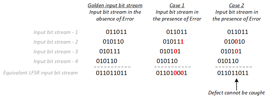
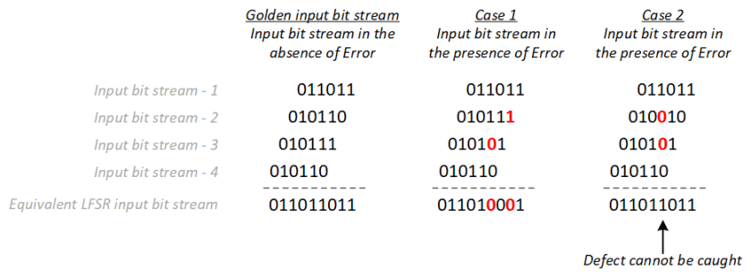
masking-in-misr-2
Leave a comment
Cancel reply
Δ
Post navigation
Published in
masking-in-misr-2
Comment
VLSI Tutorials
Sign up
Log in
Copy shortlink
Report this content
Manage subscriptions