This is article-1 of how to define Synthesis timing constraint
The objective is to define setup timing constraints for all inputs, internal and output paths.
Suppose we have a very simple and generic design (an IP) and we are the IP designer. It has a single clock domain; it has a combinational logic between input port and flip-flop, an internal combination logic between two flip-flops and combination logic between flip-flop and output port. Let’s see how we can constraint this design.

Now typically our IP will be integrated with other IPs in a SoC (as shown in Figure 2). So the input to our IP will be coming from another IP, in this case from IP-2 and the output from our IP will be going to another IP, in this case to IP-3.
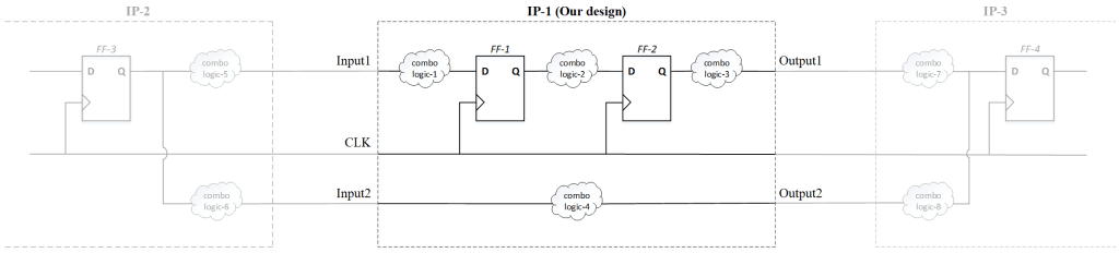
Note : After defining the input and output constraints, by default the synthesis tool assumes the input data arrives from a pos-edge clocked device prior to our design (i.e. from IP-2) and the output data goes to a pos-edge clocked flip-flop in the subsequent design (i.e. to IP-3)
Before we learn about how to apply timing constraints to input, internal or output paths, we need to first understand the definition of a path. When a synthesis tool perform timing analysis, it break the design into timing paths. A timing path has a startpoint and an endpoint, discussed below are the possible startpoints and endpoints of a timing path.
Startpoint
- Input port (other than a clock port)
- Clock pin of flip-flop
Endpoint
- Output port (other than a clock port)
- Any input pin of a flip-flop (other than a clock pin)
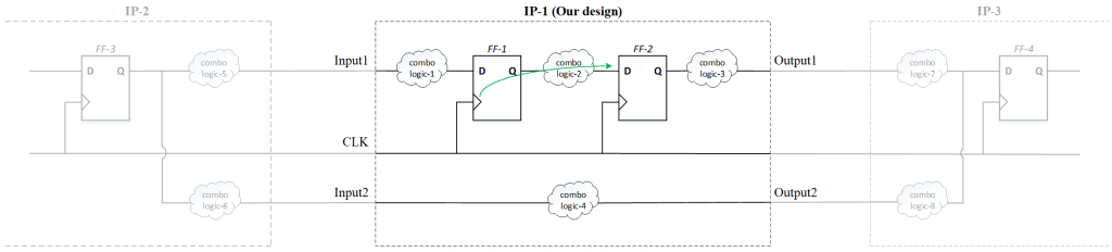
Applying these definitions, let’s look an example (Figure 3)

Path 1: Starts from an input port and ends in an input pin of flip-flop.
Path 2: Starts from a clock pin of flip-flop and ends in an input pin of flip-flop.
Path 3: Starts from a clock pin of flip-flop and ends in an output port.
Path 4: Starts from an input port and ends in an output port.
Now let’s go back to our design.
First we will focus on constraining register-to-register path –
For constraining register-to-register paths for setup time, we only need to provide the clock period to the synthesis tool. Defining the clock in a single-clock design constrains all timing paths between registers for a single cycle setup time analysis. Assume the clock in our design is having a time period of 5ns, so we will define a clock with 5ns time period and specify clock port in the design.
create_clock -period 5 [get_ports CLK]
Note: Unit of time is 1ns in this example.
Note: Synthesis tool assumes the clock rises at zero ns with 50% duty cycle, by default.
Question – 1: Suppose in our design, both flip-flops (FF-1 and FF-2) are from the same technology library, having a clock-to-Q delay of 0.5ns and setup time of 1ns. What is the maximum possible delay that can be introduced by the combination logic between the two flip-flops (combo logic-2), if we don’t want to violate the setup time? Given the time period of clock is 5ns. [Answer is 3.5ns, for the solution refer the end of this article]
In synthesis tool, clocks have ideal behavior, meaning zero rise/fall time and zero skew (as in pre-layout synthesis no clock tree synthesis is there). Estimated skew and transition time can, and should be modeled for a more accurate representation of clock behavior and therefore a more realistic timing analysis.
Modeling clock skew
Uncertainty (clock uncertainty) models the maximum delay difference between the clock network branches, known as clock skew. But it can also include non-ideal behaviors of clock like clock jitter and margin –
set_clock_uncerainity -setup Tu [get_clocks <clock>]
Example –
create_clock -period 5 [get_ports CLK]
set_clock_uncertainty -setup 0.75 [get_clocks CLK]
Modeling transition time
We need to model the rise and fall times of the clock waveform at the flip-flop clock pins –
set_clock_transition -max Tt [get_clocks <clock>]
Example –
create_clock -period 5 [get_ports CLK]
set_clock_transition -max 0.1 [get_clocks CLK]
Next we will constrain the Input1 path –
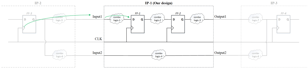
To constrain all the input paths in our design for setup time, in addition to the clock, we must provide the latest arrival time of the data at the input ports relative to the launching flip-flop’s clock edge (the time delay is called the input delay). In our example, the launching flip-flop is from IP-2, thus the input delay is the sum of clock-to-Q delay of FF-3 and the delay due to combo logic-5.
Suppose the designer of IP-2 told us that the latest arrival time at port Input1, after the FF-3 launching clock edge is 1.5ns, then we can model the same for our design using –
set_input_delay -max 1.5 -clock CLK [get_ports Input1]
Question – 2: For an input delay of 1.5ns at port Input1, what is the maximum possible delay that can be introduced by the combination logic between the port Input1 and FF-1 (combo logic-1), if we don’t want to violate the setup time? Given the setup time of FF-1 is 1ns, time period of clock is 5ns, clock uncertainty is 0.75ns and clock transition time is 0.1ns. [Answer is 1.65ns, for the solution refer the end of this article]
Then we will constrain the Output1 path –
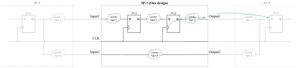
To constrain all the output paths in our design for setup time, in addition to the clock, we must provide the latest arrival time of the data at the output ports with respect to the capturing flip-flop’s clock edge (the time delay is called the output delay). In our example, the capturing flip-flop is in IP-3, thus the output delay is the sum of setup time of FF-4 and the delay due to combo logic-7.
Suppose the designer of IP-3 told us that the required latest arrival time at port Output1, before FF-4 capturing clock edge is 2ns, then we can model the same for our design using –
set_output_delay -max 2 -clock CLK [get_ports Output1]
Finally let’s constrain the port-to-port combinational path –
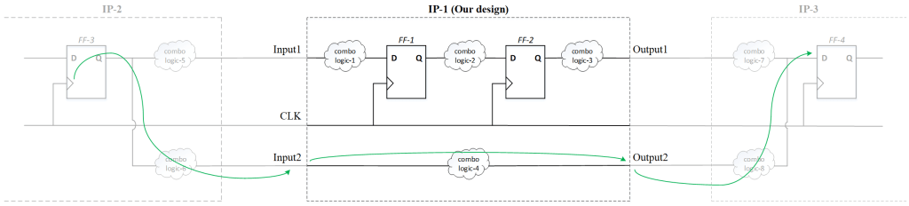
We can constrain the pure combinational path using the input delay and output delay.
Example –
set_input_delay -max 2 -clock CLK [get_ports Input2]
set_output_delay -max 2.5 -clock CLK [get_ports Output2]
Constraining a purely combinational design

Suppose we have an IP having combinational circuits only (thus no clocks in our design). Well we can still use set_input_delay and set_output_delay to constrain our inputs and outputs, because these constrains are simply modeling the delay in IP-2 and IP-3; but these are with respect to a clock. So how do we define a clock, if there is no clock in our design? The answer is virtual clock. The virtual clock is a clock that is not connected to any port or pin within the current design but instead serves as a reference for input or output delays.
create_clock -name VCLK -period 5
Now constrain our design with respect to this virtual clock.
set_input_delay -max 2 -clock VCLK [get_ports Input2]
set_output_delay -max 2.5 -clock VCLK [get_ports Output2]
But you may think, why we are discussing this! Because in practical we will never have a purely combinational logic IP. That is true, but what if this is the case (notice the clock of the FF-5 and FF-6; we don’t have CLK-2 in our design ) –

Time Budgeting
In all the examples above, we have assumed the input delay and output delay is provided to us by the other IPs’ designers, but in reality this is not the case because it is a very cumbersome task with IPs having large number of ports and also by doing so, the IPs become interdependent.
Instead we take advantage of the fact that IP-2’s output logic (combo logic-5) and our design’s input logic (combo logic-1) or our design’s output logic (combo logic-3) and IP-3’s input logic (combo logic-7) is always constrained by a full clock period; in other words the sum of delays for both the cases should be equal to or less than the time period.
So we create a time budget, meaning we allocate an appropriate portion of time period between our IP and other IPs. At first we may assume, we can use the 50-50 rules, i.e. every IP gets half a period to close the time, but this doesn’t leave any room for error. So a better approach is to allocate a number lesser than 50% for each IP, so that there is some portion of time period left to accompany any unanticipated delay.
Solutions
Answer – 1: For satisfying setup time –
(clock-to-Q delay of FF-1 + delay due to combo logic-2) ≤ (time period of clock – setup time of FF-2)
Thus, (delay due to combo logic-2) ≤ (time period of clock – setup time of FF-2 – clock-to-Q delay of FF1)
Implies, (delay due to combo logic-2) ≤ 3.5
Thus maximum possible delay that can be introduced by the combo logic-2 is 3.5ns.
Answer – 2: For satisfying setup time –
(Input delay of port Input1 + delay due to combo logic-1) ≤ (time period of clock – setup time of FF-2 – clock uncertainty – clock transition time)
Thus, (delay due to combo logic-1) ≤ (time period of clock – setup time of FF-2 – clock uncertainty – clock transition time – Input delay of port Input1)
Implies, (delay due to combo logic-1) ≤ 1.65ns
Thus maximum possible delay that can be introduced by the combo logic-1 is 1.65ns.
