In this article we are going to discuss about four types of JTAG Data Registers –
1. Boundary Scan Register (BSR)
2. Bypass Register (BR)
3. Device ID Register
4. User Data Register(s)
Before discussing about the Boundary Scan Register, it is important to understand why we need it.
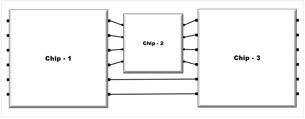
Consider a case where we have 3 chips from different vendors and we want to assemble it on one board. Assume the 3 chips have already been tested by the respective vendors using Automatic Test Equipment (ATE). But when we put them together on a board, there are chances of faults in the interconnections between the chips, then how are we going to detect that? We cannot take our board to the ATE and test all the chips again only for the purpose of testing the interconnections (ATE is highly expensive).
In the example shown in Figure 1, the Inputs/Outputs of Chip-2 is not an I/O at the board level after it is assembled. What if we want to access Chip-2’s I/O for some debug reason, then how are we going to do that?
Boundary Scan Register (BSR)
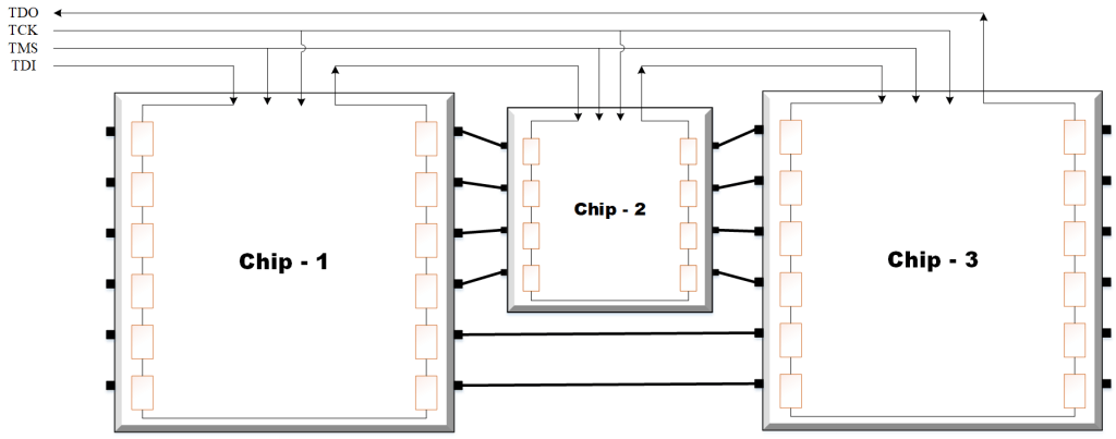
The Boundary Scan Registers solves these problems. If all the 3 Chips has JTAG in it and supports Boundary Scan, we can control and observe any device’s I/O pins even if its I/O pins are not exposed to the top. Similar to the concept of Scan and ATPG, we can load the BSR to the required value and capture the response through BSR to test the interconnections between chips (this type of testing is called Boundary Scan Testing).
The JTAG interface allows for several devices to be connected to a single interface in a daisy chain configuration. TMS and TCK are connected in parallel; TDI and TDO are connected in a serial chain as shown in the Figure 2.
Note: We can have only one TAP at any level (Board level/Chip level/IP level). Therefore instead of having a dedicated TAP for each chip at Board Level, we have a common TAP for all the Chips.
The register consists of Boundary Scan Cells (BSC) that are inserted between the device’s core logic and the I/O pins. During normal operation these cells are invisible but in test mode the cells can be used to set and/or read values from the device’s pins.

The BSC supports four operations as shown below in the table
| Operation | Control signals | Clock | Comments | |
| Mode | Shift DR | |||
| Normal | 0 | X | N/A | Functional Mode thus BSC is transparent |
| Scan | X | 1 | Capture DR | Shift data from one BSC to another using the flop-1 of BSC |
| Update | 1 | X | Update DR | Load shifted data from flop-1 to flop-2 |
| Capture | X | 0 | Capture DR | Load data from Data Input to flop-1 |
Bypass Register
It is a single-bit register which provides a short cut from TDI and TDO. It allows devices in a circuit to be tested with minimal timing overhead. Suppose we have multiple chips connected in series as shown in Figure 4 and we want to access a particular chip, say Chip-2. Now if we follow the conventional method without the bypass register, then in order to load/unload value from the BSCs of Chip-2, we have to shift the data all the way through the BSCs of Chip-1 and Chip-3 which unnecessarily increases the loading and unloading time. To avoid this delay we have bypass register which introduces only 1 clock delay per JTAG device.
In the given example –
If we go through all the 3 chips: 12 + 8 + 12 = 32 clocks
If we bypass Chip-1 and Chip-3: 1 + 8 + 1 = 10 clocks
To bypass a Chip, we load the opcode value of the Bypass Register in the Instruction Register for the Instruction Decoder to establish a path through the Bypass Register.

Device ID Register
It is only required for Device identification. Suppose we have multiple JTAG devices with each JTAG having its own debug port or TAP. To make sure we are accessing the correct debug port, we assign a unique value (called Device ID Code) to the Device ID Register of each device. The Device ID Code value enables a user or debugger tool to identify the debug port to which it is connected.
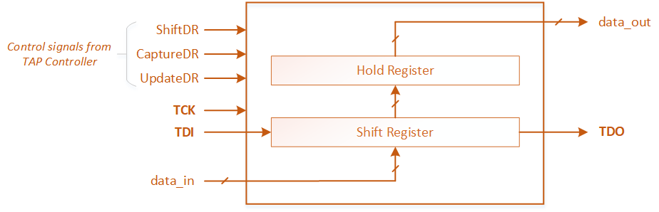
User Data Register(s)
These types of registers are required to control or observe internal registers/internal ports inside the core logic for debug purpose, as shown in the Figure 5. Typically the internal logic that we want to control through JTAG has provision to be either controlled by the Functional logic or JTAG. You can refer the example shown here to understand how we can control an internal logic using the User Data Register.

Like the Instruction Register, a User Data Register has two registers inside it as shown in Figure 6. The Hold Register stores the previous data and the Shift Register is used to shift-in the next data without affecting the stored data. The control signals to the User Data Register originates from the TAP controller and depending upon the FSM state can either cause a shift-in/shift-out through the Shift Register (serial update operation in Shift-DR state ), or cause the contents of the Shift Register to be passed across to the Hold Register (parallel update operation in Update-DR state). It is important to note that, we can have multiple User Data Registers, with each register having a unique opcode. When we load the corresponding User Data Register’s opcode into the IR, the User Data Register becomes accessible for write (or read) to control (or observe) the internal logic inside the core logic.